Semiconductor
Helping the chip industry move forward
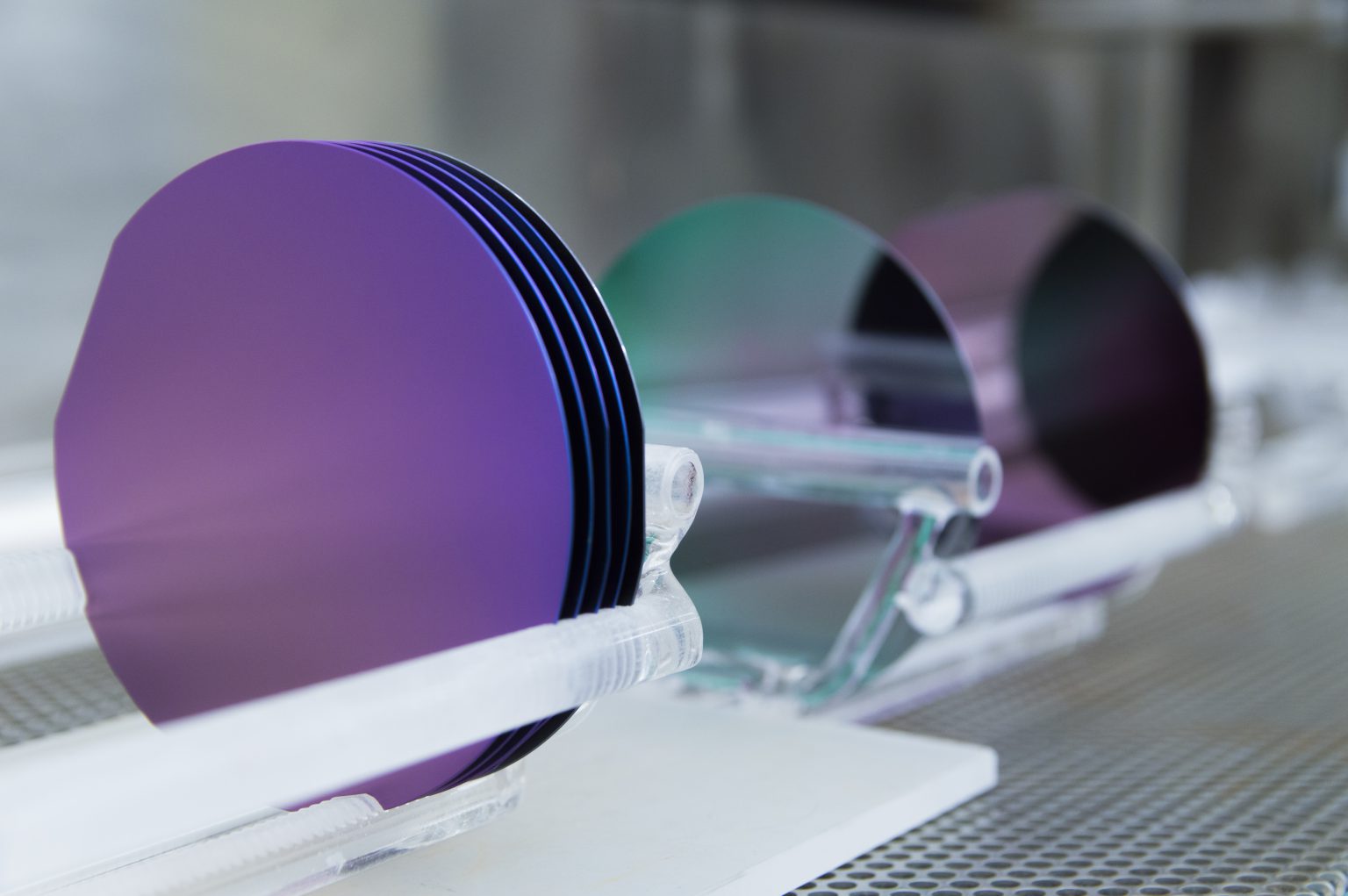
Every new generation of chips is smaller, faster and more complex than the last. The machines that make them, from DUV and EUV lithography systems to metrology equipment, have to be cleaner, more accurate and more reliable with every step. In this industry there is no room for error: a single particle can stop a production line.
What we mean for semiconductor industry
We help equipment manufacturers keep their machines clean, stable and productive. Our solutions are small and often invisible, but they protect the processes the entire chip industry depends on. Because we develop together with our customers, we grow along with their roadmap and are ready for the next generation of technology before it arrives.
What we already do
Since 2002, we have worked with leading semiconductor equipment makers. Our ultra-thin seals and foils are used in front-end lithography (DUV and EUV), photomask and pellicle, reticle applications, and metrology systems. They keep out particles and fluids, protect sensitive surfaces during production and maintenance, and can be removed without leaving residue. Every part is laser cut to an accuracy of one micron and produced in cleanrooms up to ISO class 5. We also build micron-level bonding for these machines.
Why semiconductor companies work with us
- More than twenty years of experience in the semiconductor industry
- Laser cut to 1 µm accuracy, designed to work right the first time
- Low outgassing and residue-free, suitable for vacuum and cleanroom use
- Clean, reliable and repeatable, from prototype to series
- A development partner, not just a supplier
Discuss your application
Tell us what you are working on. Our specialists will think along with you.